By Guest Authors: Johan Euphrosine and Ethan Mahintorabi @ Google
Today, Google is announcing the expansion of our partnership with SkyWater Technology. We are working together to release an open source process design kit (PDK) for SKY90-FD, SkyWater’s commercial 90nm fully depleted silicon on insulator (FDSOI) CMOS process technology. SKY90-FD is based on MIT Lincoln Laboratory’s 90 nm commercial FDSOI technology, and enables designers to create complex integrated circuits for a diverse range of applications.
Over the last two years, Google and SkyWater Technology have partnered to make building open silicon accessible to all developers, starting with the open source release of the SKY130 PDK and continuing with a series of no-cost manufacturing shuttles for developers in the open source hardware ecosystem. To date, Google has sponsored six shuttles on the Efabless platform, manufacturing 240 designs from over 364 community submissions. This is the first partnership of its type ever launched, and the results to date have been impressive.
 |
The latest MPW-6 shuttle received 90 submissions from a diverse community across 24 different countries:
Over the coming months, we'll work closely with SkyWater Technology to release their new SKY90-FD PDK under the Apache 2.0 license and organize additional Open MPW shuttles to manufacture open source designs for this new 90nm FDSOI technology, through the Efabless platform.
We believe that having access to different technologies through open source PDKs is critical to grow and strengthen the open silicon ecosystem:
- Developers can go beyond the constraints of their familiar process nodes and explore different performance, power and area trade offs with existing or new designs.
- Researchers can reproduce their research on different technologies to produce diverse figures of merit.
- Tool maintainers can generalize their technologies' backends to support more than one process.
- The community can refine the ways we structure, distribute and maintain these PDKs.
SKY90-FD is a 90nm FDSOI process. Unlike a traditional CMOS BULK process, SKY90-FD features a thin layer of insulator material between the substrate and the upper silicon layer. This thin oxide process allows the transistor to be significantly thinner than in the BULK process, allowing the device to be “fully depleted,” and simplifying the fabrication process. This extra insulation greatly reduces parasitic current leakage and lowers junction capacitances, providing improved speed and power performance under various environmental conditions.
 |
|
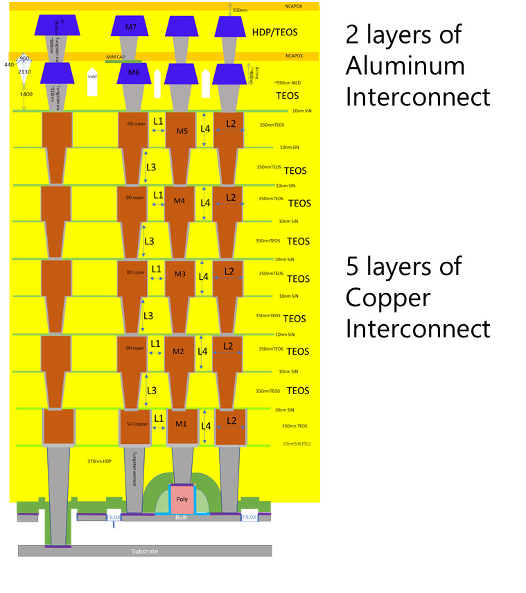
The SKY90-FD process stack topology features 5x thin Copper base metal layers for the main interconnect and two extra thicker Al (Aluminum) metal layers capable of conducting higher current. |
Google is excited about the new range of applications this open source PDK will enable once it's released later this year, and we can't wait to hear from you and watch the growing stream of innovative project ideas originating from the open silicon community.
In the meantime, make sure to check https://developers.google.com/silicon for resources and pointers to start your open silicon journey!


