By Guest Authors: Ethan Mahintorabi, Johan Euphrosine and Aaron Cunningham @ Google
Furthering Google’s goals to improve access to semiconductor technology, this agreement will provide academic researchers with unprecedented resources from a semiconductor foundry to enhance research into the physics of semiconductors and nanodevices. This includes their chemistry, defects, electrical properties, high frequency operation, and switching behavior, while reducing overall costs through economies of scale. Most importantly, this access enhances the technology transfer process by enabling researchers to develop new and emerging technologies using foundry resources, that can then be seamlessly transitioned into mass production since universities will already be using an industrially relevant platform. This will greatly improve scientist’s ability to move their technologies through the tech-transfer “valley of death” and into practical use.
Nanotechnology research has benefitted from silicon wafers that are normally used for chip manufacturing in a unique way. Instead of turning them into packaged microchips, their smooth, planarized surface makes a great substrate for building and testing nanoscale structures. This likewise helps test their transition into mass production.
 |
|
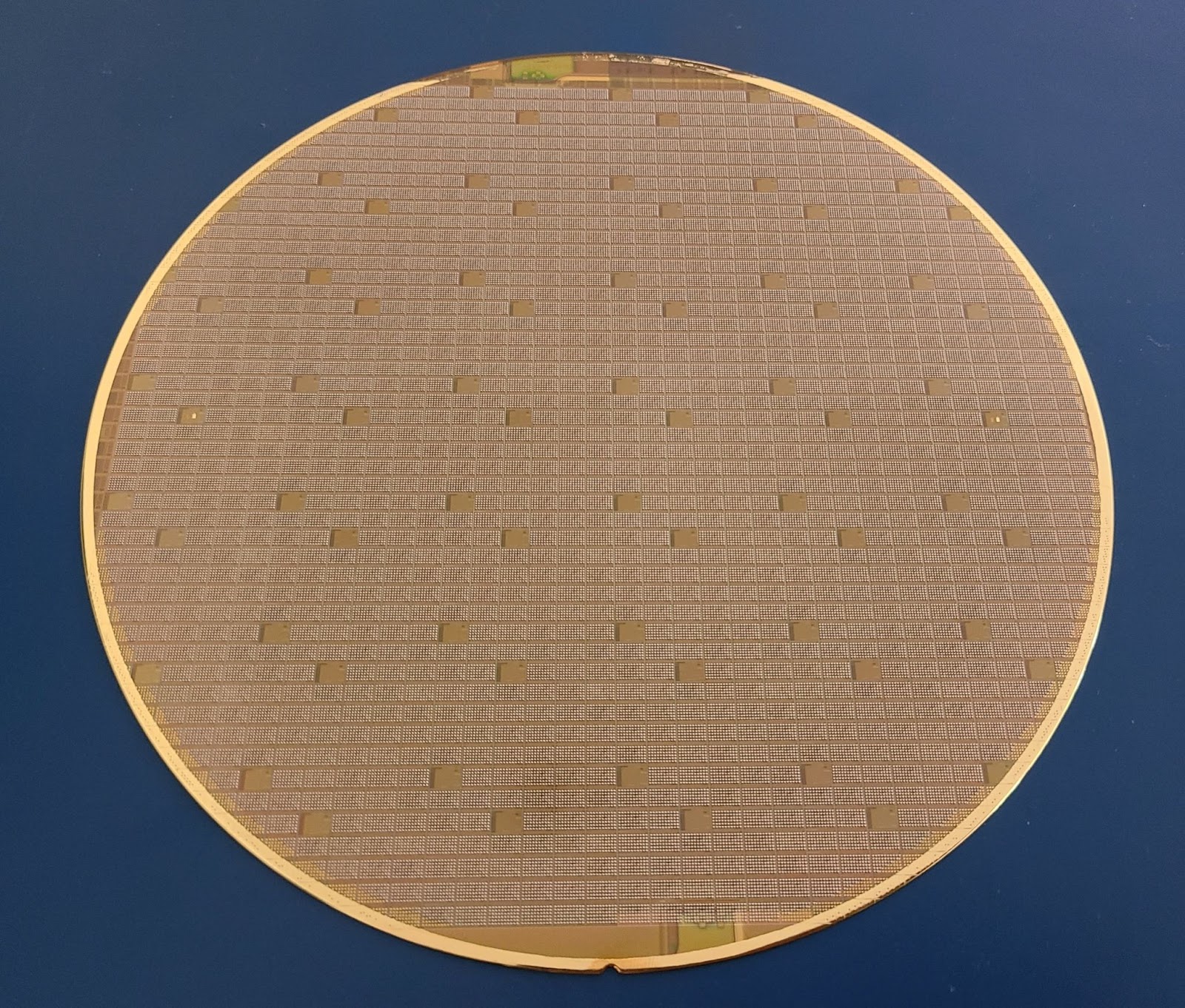
Picture of a full wafer using the SKY130 open source PDK.
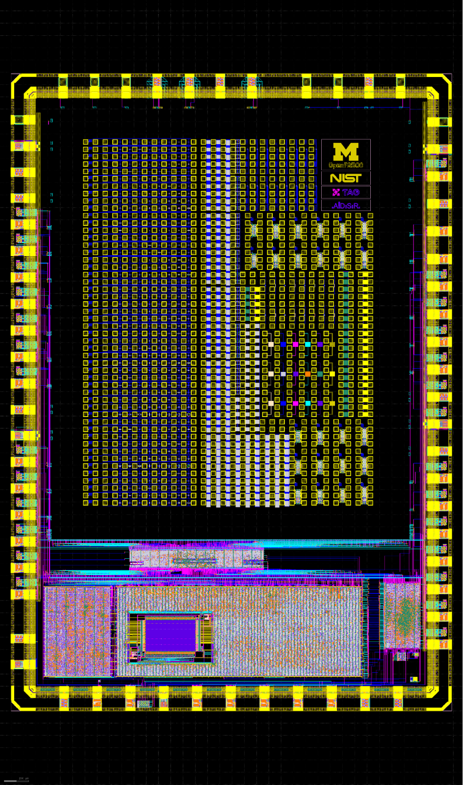
The wafer for this platform has a number of different metrology structures, from parametric test structures based on simple transistor arrays—which can be probed in a probe station—to thousands of complex measurements that users can operate using synthesized digital circuits. Critically, the wafers will be available to universities in a 200 mm form factor, and mid-production planarized wafers with less than a single nanometer of surface roughness. Smooth, flat surfaces are critical for advanced manufacturing at small sizes. NIST researchers are also ensuring that the wafers have photolithographic and electron beam alignment marks commonly found in university nanofabrication facilities, allowing the foundry silicon to be used directly by university researchers with ease. Metal pads on the surface will allow scientists to access the semiconductor transistors from the surface. NIST scientists anticipate the nanotechnology accelerator platform will enhance scientific investigations into a diverse set of technologies, including memory devices (resistive switches, magnetic tunnel junctions, flash memories), artificial intelligence, plasmonics, semiconductor bioelectronics, thin film transistors and even quantum information science. Picture of a development die from Google 's OpenMPW program for the nanotechnology accelerator developed by NIST and the University of Michigan
This program also benefits from Google’s previous contributions and support of the GDSFactory and OpenFASOC open source projects that help automate and shorten the construction of these important measuring devices from months to days. Ahead of the full wafer tapeout in 2023, NIST scientists, working with partners at the University of Michigan, Carnegie Mellon, University of Maryland, The George Washington University, and Brown University have been using Google's OpenMPW program to develop and test preliminary circuits which they expect to include in the nanotechnology accelerator. Preliminary testing will help ensure the program’s goals are met with working circuits that best serve the scientific community. A key factor in cutting-edge research is reproducibility, or the ability for researchers from different institutions to repeat each other’s experiments and improve upon them. By migrating to an open source framework, researchers can more easily share reproducible results, contribute to the creation of open source datasets to enhance future simulation, and advance the scientific community’s state of the art of nanotechnology and semiconductor manufacturing. NIST and Google will distribute the first production run of wafers to leading U.S. universities. Post-program, American scientists will be able to directly purchase the wafers from Skywater without license requirements, giving them the freedom to pursue their research without any restrictions. Since wafers are hundreds of times cheaper than full mask-sets or the cost of designing integrated circuits from scratch, scientists will have a much easier time getting and using this powerful industrial technology. Longer term, working with NIST to develop future platforms on the recently announced SKY90FD open source PDK will further expand this R&D ecosystem. To kick off this research effort NIST is organizing the "NIST Integrated Circuits for Metrology Workshop" from September 20–21, 2022. This workshop will be held online with a series of presentations and panel discussions on the first day. During the second day, a working group of researchers, scientists and engineers will work to focus on the creation of parametric test structures for monolithic integration using open source silicon technology. Visit the event website to get more details about this program and register to attend or learn more about presenting. |


